Overview
In 2014, the ECE department borrowed the idea of using a Firefly board as an interactive soldering activity to expose freshmen engineers to the Electrical and Computer Engineering Department at Bucknell. Firefly boards are designed to sync with other nearby Fireflies and blink in a rhythmic pattern, or to simply blink on their own when no other boards are nearby. With the creation of the Maker-E at the beginning of the 2015 school year, the purpose of the Firefly boards was altered to better fit the needs of the department. As with the other Makerspaces on campus, it became necessary to establish a certification process that people could complete in order to safely and correctly operate the equipment within a space. The Firefly boards were adopted to fill this niche for the Maker-E. The creation of a board requires using the majority of the equipment within the Maker-E. As students (or professors) progress through each step within the PCB process, along the way they will be making their own Firefly board. The other half of the Firefly project was constructing a placement board to stick completed Fireflies on so that they may interact with each other in different patterns to form an artistic piece for the Maker-E. As more people complete the various certifications, more Fireflies will be added to the placement board.
Process
Construction of a Firefly PCB lends itself to 3 main steps, of which certifications were developed for each: PCB design using the NI suite of Multisim and Ultiboard, milling, and soldering. Other software could be used to do PCB design, such as Altium Designer, but due to the steep learning curve associated with the Altium, Multisim and Ultiboard were selected for use.
The first step in this project was modifying the schematic being used to fit the new design that was imagined. Previously, the Firefly was implemented on a square PCB that was manufactured out-of-house. In order to realize the triangle design that we decided to use, we had to remove a few of the components in the older schematic. Following modifications of the schematic, the next step was to design the actual layout of the PCB using Ultiboard. Ultiboard was the first major learning point for this project. Both myself and Joe had previous experience using Multisim, but had very limited exposure to Ultiboard. Additionally, the work being done in Multisim was just schematic design, which is something that we had seen extensively in our classes. Ultiboard on the other hand presented new topics with important steps to adhere to that we had never been aware of before. Some of these points were Bucknell-specific. For example, traces going to surface mount components had to be located on the copper top, while traces going to through hole components were required to be on the copper bottom. Specifically for the mill in the Maker-E, you should always avoid placing a trace with a right angle. Other important learning points were more general to the realm of PCB design, such as having to make a footprint for a part before creating a custom component, or strategically placing components and traces to minimize the number of vias and the overall complexity of the board. It took multiple iterations of designing, milling, and soldering the board before all of these were learned.
Once an initial design for the Firefly circuit was achieved, the next step was to mill the schematic onto a copper clad board. We ended up milling many different iterations of the board. A large part of this was due to the lack of insight that we had regarding how to fix errors on a PCB. For example, before I knew that the purpose of the Hot Air Rework Station, if a component got moved inadvertently during some part of the soldering process, I would mill a totally new board and start from scratch, which added an incredible amount of overhead onto the process. The milling process was very straightforward, even though using the mill within the Maker-E could be frustrating at times, especially when bits broke or it was necessary to remill a section of the board multiple times before traces were completely etched. Learning the steps needed to mill correctly came easily due to the number of times we milled different Firefly boards.
After milling came soldering the surface mount and through hole components using the Pick-and-Place, reflow oven, and soldering iron. A huge learning point here was that surface mount components are far superior to through hole components and should be used whenever possible. It is so much easier to dab on solder paste and then stick the PCB into a reflow oven as opposed to having to do all of the soldering with an iron in hand. At some point after retrieving a board from the oven we were informed of the purpose of the Hot Air Rework Station which is a godsend when it comes to fixing soldering errors. Throughout this portion of the project I realized how little I really knew about good soldering practice. The creation of the soldering certification provided me with the perfect opportunity to research good technique and really improve my skills in this realm. I am now totally confident in my ability to solder a surface mount or through hole component, and can gracefully remove or fix any errors.
The final step in constructing the Firefly was testing it to make it work. Throughout the curriculum that I have experienced here at Bucknell, we have never really stressed using PCBs in any of our labs or classes. For that reason, it took some time in figuring out how to debug a PCB to determine what parts were working and which were faulty. Probably the biggest mistake to be aware of when making a PCB is bridges. These can be exceptionally small and easy to miss and will frequently be overlooked by the naked eye. The key to being able to probe a PCB is attaching many test points to the circuit. Luckily we were told about this tip early on, so when it became time to seriously debug the PCB, we were able to easily hook up different portions of the circuit to an oscilloscope. In the end, we ended up arranging the RGB LED incorrectly which burnt out one of the colors within the LED, and there was a minor bridge that we were easily able to carve away.
Results
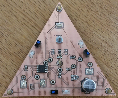
The final design of a Firefly PCB. Notice the inclusion of 5 test points for easy debugging. The Firefly is powered by a central spring-loaded pin for power and 3 outer spring-loaded pins for ground. The magnet is used to hold a Firefly to the placement board.
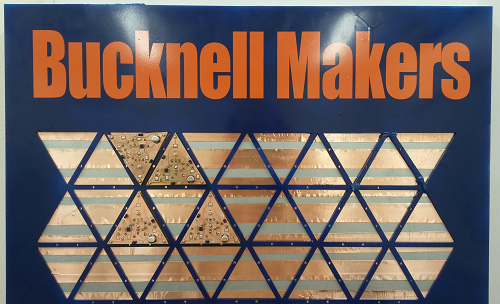
The placement board with multiple Firefly boards on it at the same time.
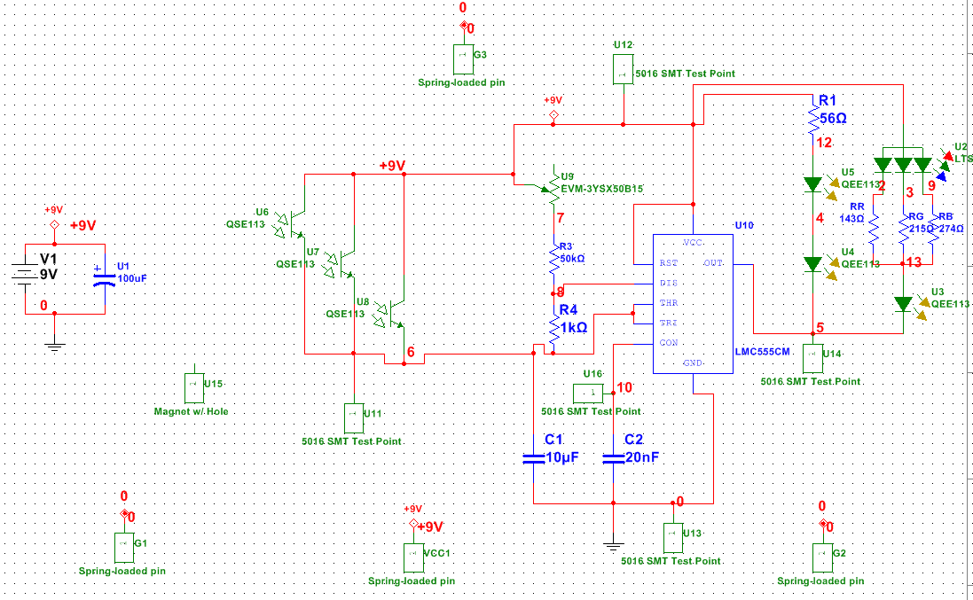
Final Firefly schematic.
Related Files